OKI WORLDWIDE
CONTACT
SITEMAP
JAPANESE SITE
SERVICES
ABOUT US
SERVICES
ABOUT US
SITEMAP
JAPANESE SITE
OKI WORLDWIDE
Close
Home
Services
List of Service
Each link moves to a Japanese Site
Service(Each link moves to a Japanese Site)
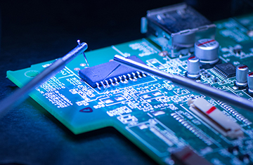
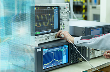
Reliability evaluation of devices/modules, electrical characteristic measurement and evaluation
ESD testing and TLP measurement
Analysis (failure/good product), observation, and examination
Chemical analysis (RoHS, REACH, environmental)
Technical and environmental information research services for electronic components
Environmental system technology
Reliability Evaluation Testing, Environmental Testing
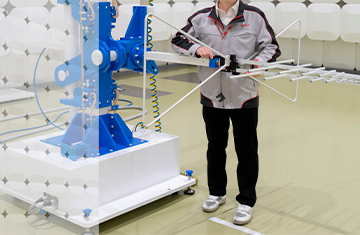
EMC testing
Instrument calibration
ページの先頭へ
See More
Pickup Contents